Introduction to SEM Analysis and Its Role in Industry
Scanning Electron Microscopy with Energy-Dispersive X-ray Spectroscopy, or SEM-EDX analysis Chennai is a high-resolution and accurate imaging technique that analyzes particle shapes and composition of materials at the nanoscale. The technique is used to detect material characterization, contamination checks, and defect analysis. From pharmaceuticals to electronics and from quality control to material development, SEM-EDX determines the elemental composition of the material and evaluates material performance and further improvements.
Common Material Defects Faced by Chennai Industries
Some of the material challenges faced by Chennai industries include:
- Defects in casting and welding
- Delamination of metal plates
- Surface defects, inclusions and surface blemishes
- Debonding and fibre misalignment
- Porosity, cracks and fissures
- Microstructural defects
- Atomic and crystalline defects
How SEM Analysis Detects Micro-Level Defects
The testing sample is bombarded with an electron beam that emits X-rays. The energy of these rays gives information about the elemental composition of the sample. In the EDX method, energy-dispersive X-ray spectroscopy is used to detect chemical characterization and composition. The use of X-ray makes it a powerful tool, allowing it to trace and map the elemental orientation of the sample.
Role of SEM-EDX in Identifying Elemental Composition
SEM testing services in Chennai use a combination of SEM and EDX to identify the elemental composition of any given sample.
- It helps to identify the presence of impurities in any compound.
- The method allows for qualitative and quantitative analysis of any sample.
- SEM-EDX is beneficial in identifying failures and defects.
- Beneficial in understanding alloy composition, coating examination, and coating flaws.
SEM Analysis in Failure Analysis and Root Cause Identification
- SEM-EDX analysis offers magnification up to 1,000,000x, allowing detection of microfractures and surface boundaries.
- SEM analysis for manufacturing industries in Chennai can identify contaminants or diluted material composition before the final product is manufactured.
- The technique can examine a fracture surface and determine whether the failure is ductile, brittle or fatigue-related.
Industries in Chennai Benefiting from SEM Analysis
SEM analysis boosts reliability and ensures regulatory compliance. The analysis finds its application in the following industries:
- Automotive industry- Investigates wear and tear and fractures in components.
- Electronics and communication: helps with micro-crack detection and solder joint inspection.
- Pharmaceuticals- Enables to detect surface integrity and medicine contaminants.
- Manufacturing- The analysis is beneficial in product development and ensuring product quality.
Apart from these, other industries that utilise SEM-EDX analysis in Chennai include food and packaging, petrochemical, geology, and materials science.
Advantages of SEM Analysis Over Conventional Testing Methods
Conventional testing methods have drawbacks and do not fit modern analysis and characterisation. Here is why SEM analysis is advantageous over traditional methods:
- Better magnification capabilities and nanoscale imaging reveal intricate structural details that are nearly impossible to achieve with conventional methods.
- SEM images offer a 3-D representation with a large depth of field for samples.
- The analysis can also detect uneven surfaces accurately.
- The method is versatile and can be applied to a wide range of industries.
- Minimal human error, automated operations, and quantitative analysis make SEM a better option over optical microscopy and basic physical inspections.
Real-World Industrial Applications of SEM Analysis
One can find real-world applications of SEM analysis in the following industries:
- Oil and gas industry
- Electronics and semiconductor industry
- Medical and life science industry
- Food and beverages industry
- Material science industry
Why Choose a Professional SEM Testing Lab in Chennai
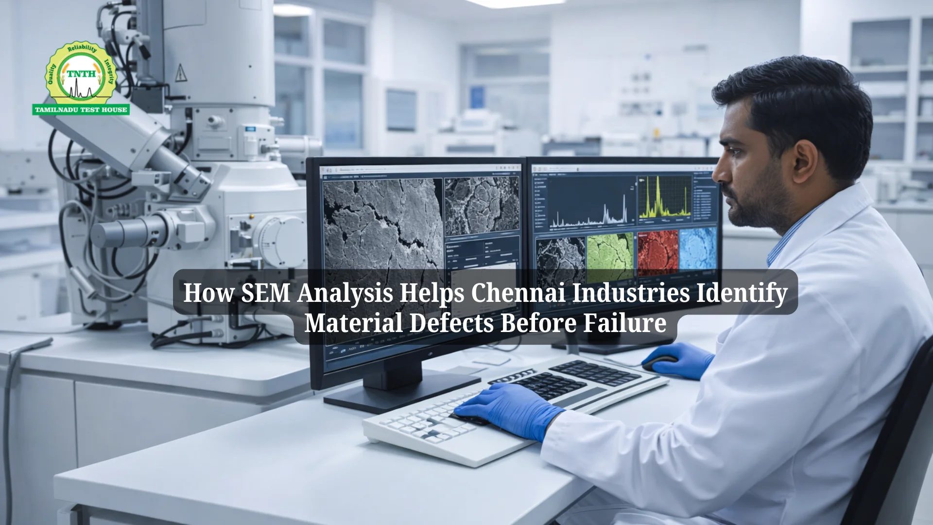
Going to a professional test lab for SEM analysis provides clear test results, detailed reports, and expert assistance. Tamil Nadu Test House offers industrial material testing in Chennai for all your material testing needs. Our state-of-the-art lab is equipped with advanced SEM technology that ensures quality and transparency. Our advanced lab has vast experience in working with industries like automotive, pharma, electronics, and geoscience. Moreover, our SEM reports include high-resolution SEM images, EDX spectra, element maps, and composition tables, along with expert notes.
Conclusion: Preventing Costly Failures Through Early Defect Detection
We are a growing testing laboratory for SEM-EDX analysis in Chennai that promises the latest technology, highly skilled scientists, and fast turnaround times. Rely on the best test house near you and build a legacy of trust, innovation, and security.