
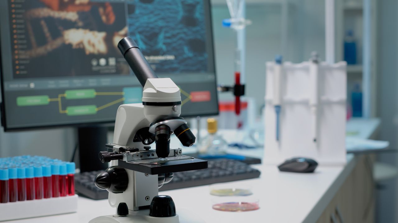
SEM EDX Analysis (Scanning Electron Microscopy with EDX)
Scanning electron microscopy (SEM) with energy-dispersive X-ray spectroscopy (EDS or EDX) generates a sharp picture of the sample’s microscopic surface structures and provides information about its elemental composition. SEM-EDX analysis is suitable for almost all sample types and has a vast number of applications from basic scientific research to product development and quality control.
What is SEM-EDX used for?
SEM-EDX has many applications in industrial manufacturing and materials science. It can also be used for energy and resource management, as well as for the examination of consumer-packaged articles. With SEM-EDX, large, heavy, and challenging samples can be examined with excellent image quality showing the smallest details and the chemical composition of the material’s surface.
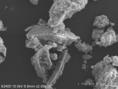
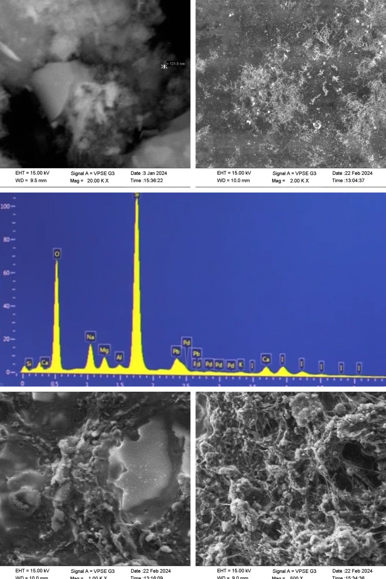
In product development, SEM-EDX is commonly used for failure and defect analyses and process characterization. Particle type and size determination and material classification can also be performed with the help of SEM-EDX to ensure the quality of the product and optimize its production processes. It is also possible to perform reverse engineering and breaking mechanism analyses.
Elemental mapping, where different elements and compounds detected by the EDX detector are marked with different colors in the picture, is an effective method for observing the elemental composition of a sample at a glance. SEM-EDX can also help determine if the produced material has some additional substances, and at which point of the manufacturing process they have ended up in it.
Deeper structural analysis of different materials, including the examination of surface topology, detection of surface contamination as well as determination of the causes of chemical reactions, such as corrosion and oxidation with the help of SEM-EDX can also be very useful for research and development work.
How does SEM-EDX work?
With SEM, the microscopic surface structures of the sample can be observed with high precision. A scanning electron microscope typically has a resolution in the nanometer range, which is much higher than that of a traditional light microscope.
Therefore, a more accurate image of the sample’s surface topography is obtained with SEM. More information about the SEM operating principle can be found on our SEM page.
A large selection of needs in science and industry can be met with SEM, as many different accessories can be added to the microscope to get different kinds of information about the sample (e.g. EBSD, BSE).
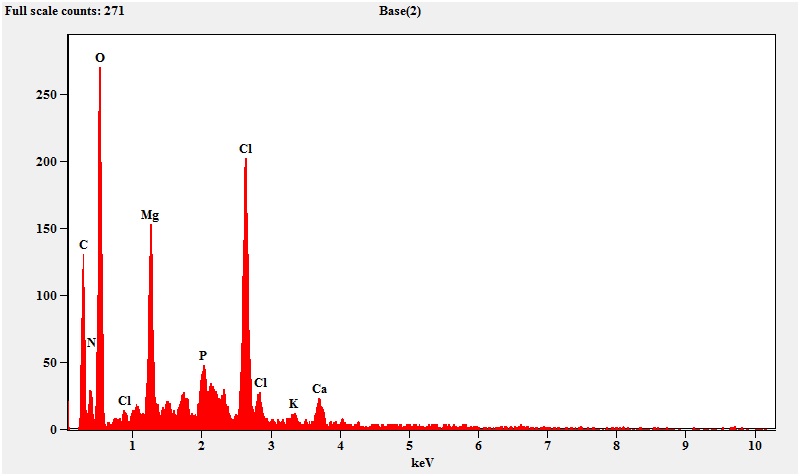
When the goal is to determine the elemental composition of the sample, an additional EDX detector is attached to the SEM machine. The EDX detector identifies the elements in the sample along with determining their concentrations and distribution.
For more information about our SEM analysis capabilities or to request a quote, Please mail us at [email protected]
SEM vs EDX
Scanning Electron Microscopy (SEM) and Energy Dispersive X-ray Spectroscopy (EDX) are complementary techniques used for material characterization. SEM produces high-resolution images to study surface morphology, particle shape, structure and microscopic defects. EDX identifies the elemental composition of a selected area of the sample. In simple terms, SEM shows what the surface looks like, while EDX helps determine which elements are present. Combining both techniques provides valuable structural and elemental information.
What Materials Can Be Tested?
SEM EDX analysis can be applied to a wide range of solid materials, depending on the sample condition and analytical requirement. Common samples include metals and alloys, polymers, composites, powders, particles, ceramics, minerals, coatings, corrosion products, industrial components, contaminants and pharmaceutical materials. Sample preparation requirements may vary according to the material and testing objective.
SEM EDX Applications
SEM EDX is also widely used in failure analysis to identify material defects, contamination, corrosion and elemental variations that may contribute to product or component failure. It can help investigate defects, foreign particles, deposits and variations in materials by combining microscopic imaging with elemental information.
SEM EDX Elemental Analysis
SEM EDX elemental analysis identifies elements present in a selected region of a sample by detecting characteristic X-rays generated during analysis. Depending on the requirement, EDX can support point analysis, selected-area analysis and elemental mapping, helping visualize the distribution of detected elements across the examined surface.
SEM EDX Testing Services
Tamilnadu Test House provides SEM EDX testing services for surface examination, material characterization and elemental analysis. SEM-EDX testing can support investigations involving surface morphology, elemental composition, particles, contaminants, coatings, corrosion and material defects. The testing approach can be selected according to the sample type and analytical objective to obtain relevant microscopic and elemental information.